If an embedded DRAM (eDRAM) block is to be integrated into a System-on-Chip (SoC), a fundamental trade-off arises between cell density and data retention time. Identifying the optimal balance between these two parameters is essential for achieving the desired performance, area efficiency, and reliability. In the following article, this trade-off is analyzed and discussed in detail.
Author: Amin Chegeni
-
Getting Started with Open-Source CMOS Analog IC Design Toolchain
To begin working with open-source tools for CMOS analog IC design, all you need is a computer and a stable internet connection.
It is recommended to install Linux, as all of the essential tools run smoothly on Linux-based systems. Linux distributions are free, and if you are using Windows, you can easily set up a Linux environment through WSL (Windows Subsystem for Linux). For example, I am using Ubuntu on WSL.
Below are the main tools used in a typical analog IC design flow:
- Schematic Capture:
xschem — https://xschem.sourceforge.io/stefan/index.html - Circuit Simulation:
ngspice — https://ngspice.sourceforge.io - Layout Editor:
Magic VLSI — http://opencircuitdesign.com/magic/index.html - Open PDK:
SkyWater SKY130 — http://opencircuitdesign.com/open_pdks/index.html
Integrating Xschem with SKY130
There are clear instructions available for setting up xschem with the SKY130 PDK:
Documentation:
XSCHEM SKY130 INTEGRATIONA detailed video tutorial is also available, covering xschem, ngspice, and SKY130 PDK usage from scratch:
https://youtu.be/bYbkz8FXnsQ?si=K5OG5g5v23BnFscz - Schematic Capture:
-
MOSFET Small-Signal Characteristics
In this article, we extract the small-signal characteristics of MOSFETs using open-source and free available PDKs and CAD tools. The analysis is carried out using the SkyWater sky130 PDK, Xschem as the schematic capture tool, and Ngspice as the circuit simulator.
All tools (Xschem, Ngfspice, and sky130 PDK) must be installed properly on a Linux system. In this work, Ubuntu running under WSL is used. The installation procedure is discussed in a separate article.
The reader is assumed to have a basic understanding of MOSFET device physics and the fundamentals of MOSFET operation. Figure 1 illustrates the structure and symbols of NMOS and PMOS devices. In integrated-circuit design, each MOSFET has four terminals: gate (G), source (S), drain (D), and bulk (B). Modern CMOS technologies typically employ a p-type substrate; therefore, the bulk of all NMOS devices (except native devices) is tied to the substrate, i.e., GND or VSS. In contrast, PMOS devices are fabricated in isolated wells, allowing their bulks to be biased independently.
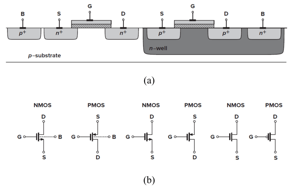
Figure 1: (a) structure of NMOS and PMOS, (b) symbols (from [1]) Operation regions:
A MOSFET behaves as a switch (ON or OFF) in digital design, but in analog design it operates in one of three regions:
- Cut-off (OFF): VGS < VTH and VGD < 0
- Saturation: VGS > VTH and VGD < VTH
- Triode (ON): VGS > VTH and VGD > VTH
Note that the transition between these regions is smooth, especially near the threshold voltage.
Voltage – Current Characteristics:
To explain MOSFET operation, we review the V–I equations of an NMOS transistor. PMOS equations follow the same form.
Triode region (ON):
For VDS << 2(VGS – VTH):
Saturation region:
Including channel length modulation,
The parameter λ is the channel-length modulation coefficient, which decreases with increasing channel length:
Second-order effects:
Body effect: Increasing the source-to-bulk voltage raises the threshold voltage:
Subthreshold (Weak Inversion) : When VGS ≈ VTH, the device enters weak inversion, and the drain current follows:
where I0 is proportional to W/L, and ξ > 1 and VT = kT/q. We say the device operates in weak inversion in contrast with strong inversion.
Small-signal model:
Fig.2 shows the small-signal MOSFET model [1].
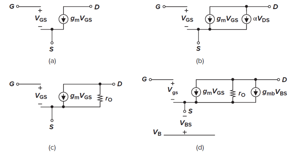
Figure 2: (a) Basic MOS small-signal model; (b) channel-length modulation represented by a dependent current source; (c) channel-length modulation represented by a resistor; (d) body effect represented by a dependent current source. [1] Equations:
In triode region, a MOSFET behaves as a voltage-controlled resistor:
In saturation, the transconductance is:
Equivalent expressions include:
The output resistance due to channel-length modulation is:
For λVDS << 1,
The body-effect transconductance is:
where η is typically around 0.25
Simulation results:
Long-channel NMOS: The circuit in fig. 3 is used to evaluate the small-signal, low frequency behavior of an NMOS device. Because capacitances are not considered in this section, DC-sweep analysis is employed.
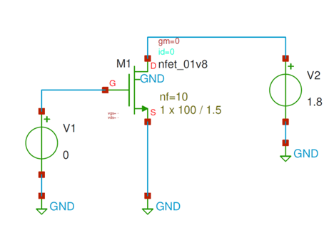
Figure 3: Simple NMOS circuit used for DC-sweep analysis Here, the W/L is 100u/1.5u, number of gates (fingers) are 10, and the VGS sweep is from 0 to 1.8V. Fig. 4 shows gm and gds of the NMOS versus VGS.
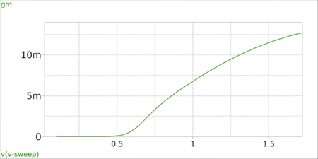
Figure 4(a) 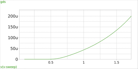
Figure 4(b) In this circuit, VTH ≈ 560mv. As expected, by increasing VGS, both gm and gds increase. It’s interesting to see the gds – ID relationship as shown in fig. 5. The curve is nearly linear, and according to (15), its slope is corresponds to the channel-length modulation coefficient λ.

Figure 5: gds vs. ID The intrinsic small-signal gain of a MOSFET is defined as
Fig. 6 plots the gain vs. VGS.

Figure 6: Intrinsic small-signal low-frequency gain of NMOS with W/L = 100u/1.5u In this example of long-channel NMOS, the gain peaks at an overdrive voltage of Vov = VGS – VTH ≈ 100 mV.
As Vov (and thus ID) increases, the gain decreases. Below Vov ≈ 80 mV, the device is in weak inversion, and for VGS < VTH, the gain loses its physical meaning.
Short-channel (sub-micron) NMOS: For channel length below 1 um (sub-micron), the MOS device behavior is significantly affected by short-channel and higher-order effects. Figure 7 illustrates how these phenomena alter the small-signal parameters for a device with W/L = 10u/0.15u. Detailed discussion of short-channel devices will be provided in a subsequent article.
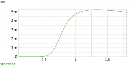
Figure 7(a) 
Figure 7(b) 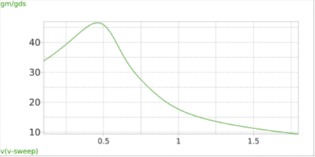
Figure 7(c) 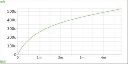
Figure 7(d) [1] Razavi, B., Design of Analog CMOS Integrated Circuits, 2nd ed. New York, NY, USA: McGraw-Hill, 2017.
-
Digital Background Calibration in Modern High-Speed, High-Resolution ADCs
With the advent of advanced nanometer CMOS technologies, there has been an unprecedented surge in the speed and capabilities of digital devices, signal processing, parallel computing, and artificial intelligence (AI). Consequently, the demand for high-speed, high-resolution data converters has risen significantly. Among various analog-to-digital converter (ADC) architectures, the pipelined ADC stands out, offering a favorable combination of high-speed conversion and moderate resolution, typically in the range of 10 to 14 bits.
However, while modern nanometer-scale processes enable the development of faster devices, they also introduce significant challenges, particularly due to the limited power supply voltage (VDD) these processes afford. This reduced voltage range complicates the design of ADC sub-blocks, as achieving the required performance within these constraints becomes increasingly difficult. As a result, designing the sub-blocks of ADCs, such as amplifiers, comparators, and sample-and-hold circuits, has become a particularly challenging task in the field.
In pipelined ADCs, the inter-stage gain stages are particularly vulnerable to the limitations imposed by low VDD. The gain stages must amplify the signal accurately while operating within a restricted voltage range, making this one of the most critical and difficult aspects of pipelined ADC design. The trade-offs between speed, power efficiency, and precision in these gain stages often determine the overall performance of the ADC, making it a crucial area for optimization.
To address these challenges, digital background calibration techniques are increasingly employed. These techniques leverage the strength of digital signal processing to compensate for analog imperfections, improving both the speed and accuracy of ADCs. Digital calibration can correct for errors such as gain mismatches, offset errors, and non-linearities, thus enabling modern pipelined ADCs to achieve the desired levels of performance even in the face of stringent design constraints.
In summary, while the evolution of nanometer CMOS technologies has enabled the development of faster ADCs, the accompanying reduction in supply voltage presents significant design challenges. In particular, pipelined ADCs, with their high-speed and moderate resolution characteristics, require careful optimization of their gain stages. Digital background calibration has emerged as a powerful tool to mitigate these challenges, ensuring that modern ADCs meet the growing demands for high-speed, high-resolution data conversion.
Digital Signal Processing (DSP) is typically performed in two well-known domains: the time-domain and the frequency-domain, each offering distinct advantages and limitations.
In time-domain DSP, the signal is processed based on its amplitude variation over time. Common operations in this domain include filtering, convolution, correlation, and windowing. Time-domain methods are straightforward and effective for real-time applications, where the evolution of the signal over time is of primary interest.
In frequency-domain DSP, the signal is transformed into the frequency domain using techniques like the Fourier Transform. In this domain, the signal is represented as a function of its constituent frequencies. Key operations, such as filtering or compression, are performed based on the signal’s frequency content. While time-domain analysis focuses on how the signal changes over time, frequency-domain methods provide a deeper understanding of the signal’s harmonic components, making it especially useful for applications like spectral analysis, audio processing, and telecommunications.
In addition to these, there is a third, less commonly discussed method called Histogram Signal Analysis. This approach involves analyzing the distribution of a signal’s amplitude values over time by creating a histogram, which plots the frequency of amplitude occurrences. Histogram analysis is based on counting—a simple and highly efficient operation in the digital realm.
One of the unique advantages of histogram analysis is its applicability to ADC error extraction and correction. For instance, it can be used to detect and correct gain errors in pipelined ADCs. This makes histogram-based techniques particularly valuable in improving the accuracy and reliability of high-speed, high-resolution ADCs.
One example is explained in my published article. Take a look at it:
-
Useful Stuff: Capacitor (part 2)
SRF:
A capacitor doesn’t always behave like a capacitor, especially at high frequencies. As shown below, the equivalent circuit of a capacitor includes a series inductance, known as the Equivalent Series Inductance (ESL). The ESL varies depending on the capacitor type, packaging, and physical dimensions.
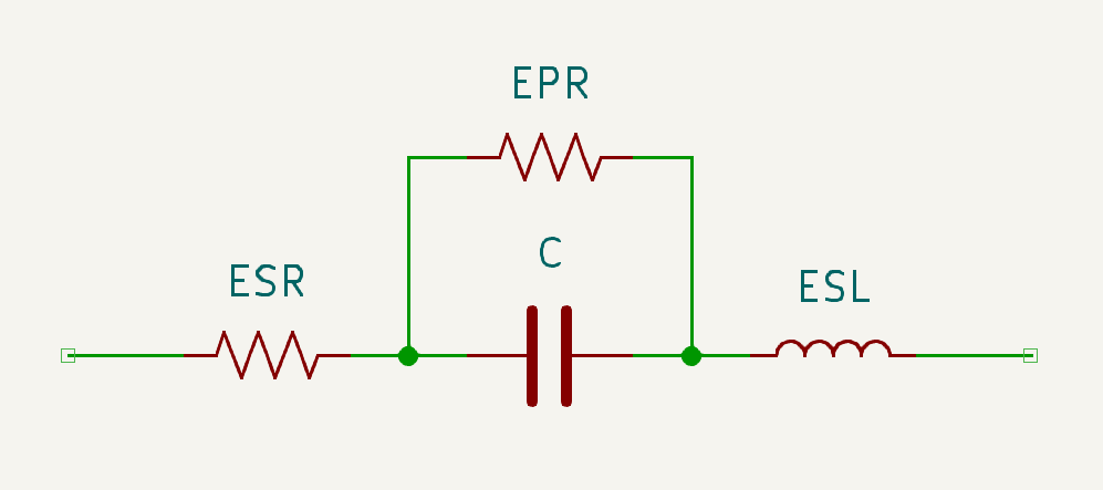
Capacitor Model At low frequencies, the impedance of the ESL (ZL) is negligible compared to the impedance of the capacitor (ZC):
As the frequency increases, ZL increases while ZC decreases. At high frequencies, the inductive impedance dominates, causing the capacitor to act more like an inductor. But what do we mean by “low frequency” and “high frequency”? How can they be distinguished?
At a specific frequency, the two impedances ZL and ZC become equal. This is known as the self-resonant frequency (SRF) of the capacitor:
Larger capacitors tend to have a lower SRF. This is why, in some cases, you may see a nano-Farad capacitor placed in parallel with a multi-micro-Farad capacitor. The smaller capacitor is used to maintain capacitive behavior at higher frequencies where the larger capacitor cannot.
