In this article, we extract the small-signal characteristics of MOSFETs using open-source and free available PDKs and CAD tools. The analysis is carried out using the SkyWater sky130 PDK, Xschem as the schematic capture tool, and Ngspice as the circuit simulator.
All tools (Xschem, Ngfspice, and sky130 PDK) must be installed properly on a Linux system. In this work, Ubuntu running under WSL is used. The installation procedure is discussed in a separate article.
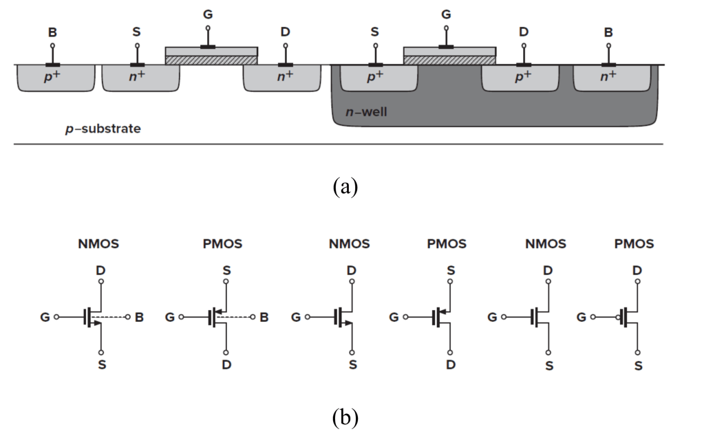
The reader is assumed to have a basic understanding of MOSFET device physics and the fundamentals of MOSFET operation. Figure 1 illustrates the structure and symbols of NMOS and PMOS devices. In integrated-circuit design, each MOSFET has four terminals: gate (G), source (S), drain (D), and bulk (B). Modern CMOS technologies typically employ a p-type substrate; therefore, the bulk of all NMOS devices (except native devices) is tied to the substrate, i.e., GND or VSS. In contrast, PMOS devices are fabricated in isolated wells, allowing their bulks to be biased independently.
Operation regions:
A MOSFET behaves as a switch (ON or OFF) in digital design, but in analog design it operates in one of three regions:
- Cut-off (OFF): VGS < VTH and VGD < 0
- Saturation: VGS > VTH and VGD < VTH
- Triode (ON): VGS > VTH and VGD > VTH
Note that the transition between these regions is smooth, especially near the threshold voltage.
Voltage – Current Characteristics:
To explain MOSFET operation, we review the V–I equations of an NMOS transistor. PMOS equations follow the same form.
Triode region (ON):
For VDS << 2(VGS – VTH):
Saturation region:
Including channel length modulation,
The parameter λ is the channel-length modulation coefficient, which decreases with increasing channel length:
Second-order effects:
Body effect: Increasing the source-to-bulk voltage raises the threshold voltage:
Subthreshold (Weak Inversion) : When VGS ≈ VTH, the device enters weak inversion, and the drain current follows:
where I0 is proportional to W/L, and ξ > 1 and VT = kT/q. We say the device operates in weak inversion in contrast with strong inversion.
Small-signal model:
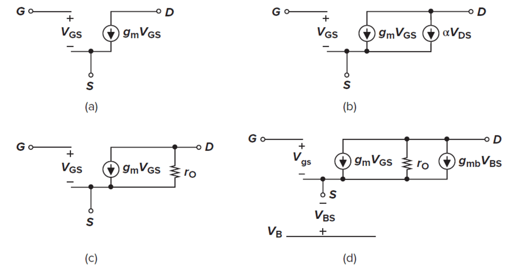
Fig.2 shows the small-signal MOSFET model [1].
Equations:
In triode region, a MOSFET behaves as a voltage-controlled resistor:
In saturation, the transconductance is:
Equivalent expressions include:
The output resistance due to channel-length modulation is:
For λVDS << 1,
The body-effect transconductance is:
where η is typically around 0.25
Simulation results:
Long-channel NMOS: The circuit in fig. 3 is used to evaluate the small-signal, low frequency behavior of an NMOS device. Because capacitances are not considered in this section, DC-sweep analysis is employed.
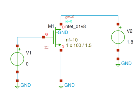
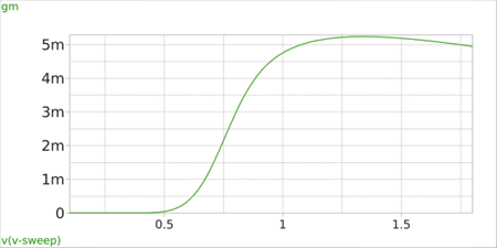
Here, the W/L is 100u/1.5u, number of gates (fingers) are 10, and the VGS sweep is from 0 to 1.8V. Fig. 4 shows gm and gds of the NMOS versus VGS.
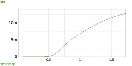
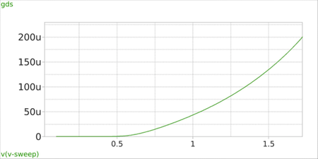
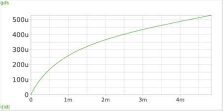
In this circuit, VTH ≈ 560mv. As expected, by increasing VGS, both gm and gds increase. It’s interesting to see the gds – ID relationship as shown in fig. 5. The curve is nearly linear, and according to (15), its slope is corresponds to the channel-length modulation coefficient λ.

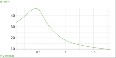
The intrinsic small-signal gain of a MOSFET is defined as
Fig. 6 plots the gain vs. VGS.

In this example of long-channel NMOS, the gain peaks at an overdrive voltage of Vov = VGS – VTH ≈ 100 mV.
As Vov (and thus ID) increases, the gain decreases. Below Vov ≈ 80 mV, the device is in weak inversion, and for VGS < VTH, the gain loses its physical meaning.
Short-channel (sub-micron) NMOS: For channel length below 1 um (sub-micron), the MOS device behavior is significantly affected by short-channel and higher-order effects. Figure 7 illustrates how these phenomena alter the small-signal parameters for a device with W/L = 10u/0.15u. Detailed discussion of short-channel devices will be provided in a subsequent article.

[1] Razavi, B., Design of Analog CMOS Integrated Circuits, 2nd ed. New York, NY, USA: McGraw-Hill, 2017.

Leave a comment